Abstract
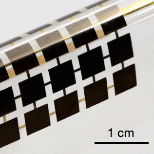
Organic–inorganic hybrid perovskites have electronic and optoelectronic properties that make them appealing in many device applications. Although many approaches focus on polycrystalline materials, single-crystal hybrid perovskites show improved carrier transport and enhanced stability over their polycrystalline counterparts, due to their orientation-dependent transport behaviour and lower defect concentrations. However, the fabrication of single-crystal hybrid perovskites, and controlling their morphology and composition, are challenging. Here we report a solution-based lithography-assisted epitaxial-growth-and-transfer method for fabricating single-crystal hybrid perovskites on arbitrary substrates, with precise control of their thickness (from about 600 nanometres to about 100 micrometres), area (continuous thin films up to about 5.5 centimetres by 5.5 centimetres), and composition gradient in the thickness direction (for example, from methylammonium lead iodide, MAPbI3, to MAPb0.5Sn0.5I3). The transferred single-crystal hybrid perovskites are of comparable quality to those directly grown on epitaxial substrates, and are mechanically flexible depending on the thickness. Lead–tin gradient alloying allows the formation of a graded electronic bandgap, which increases the carrier mobility and impedes carrier recombination. Devices based on these single-crystal hybrid perovskites show not only high stability against various degradation factors but also good performance (for example, solar cells based on lead–tin-gradient structures with an average efficiency of 18.77 per cent).
